
Semiconductors in South Korea
South Korea-India Semiconductor Partnership:
Precision Engineering Meets Massive Market
Executive Summary
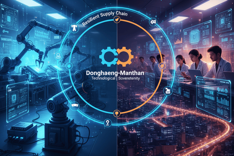
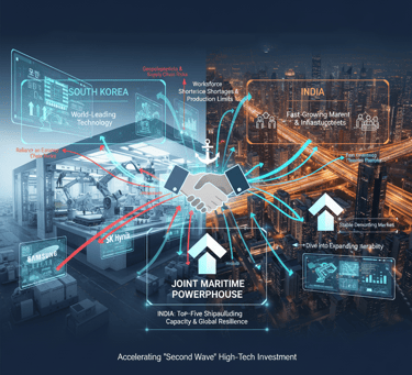
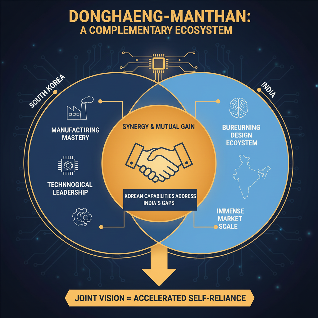
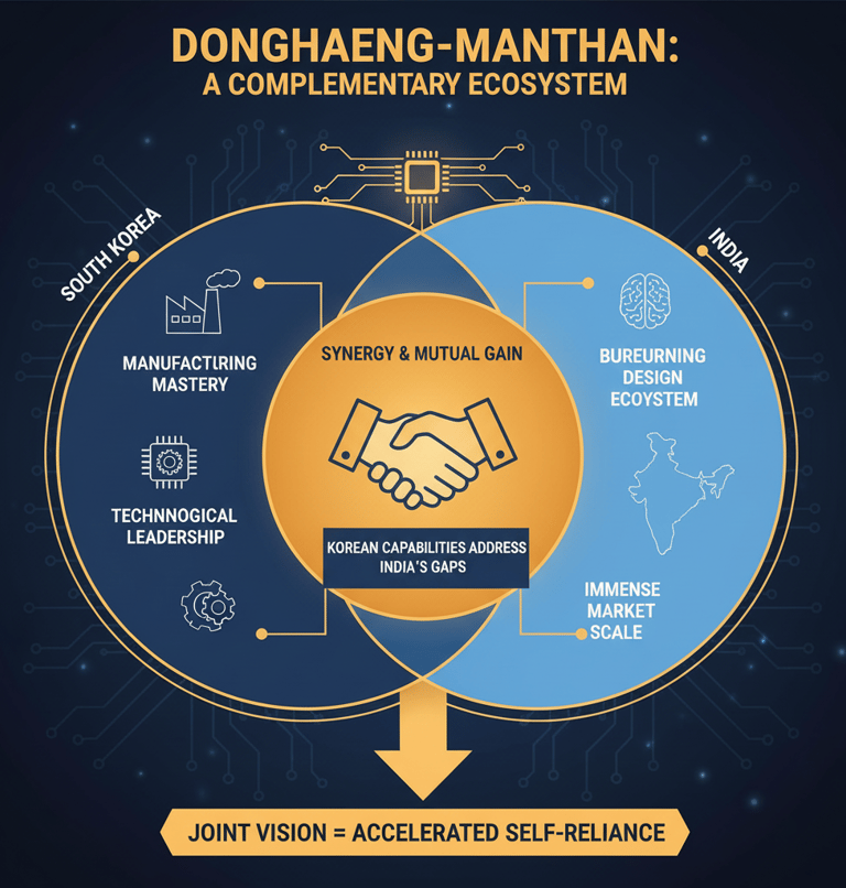
The Donghaeng-Manthan initiative forges a powerful, symbiotic partnership between South Korea and India, designed to create a resilient, vertically integrated semiconductor supply chain. This collaboration is not merely an economic opportunity but a strategic imperative, driven by geopolitical shifts and a shared vision for technological sovereignty. By uniting South Korea's world-leading precision engineering and manufacturing prowess with India's vast talent pool and market scale, this partnership is poised to redefine Asian technological leadership and secure a dominant position in the global semiconductor landscape.

Demand Shock Ahead:
India's Chip Market to Triple by 2030
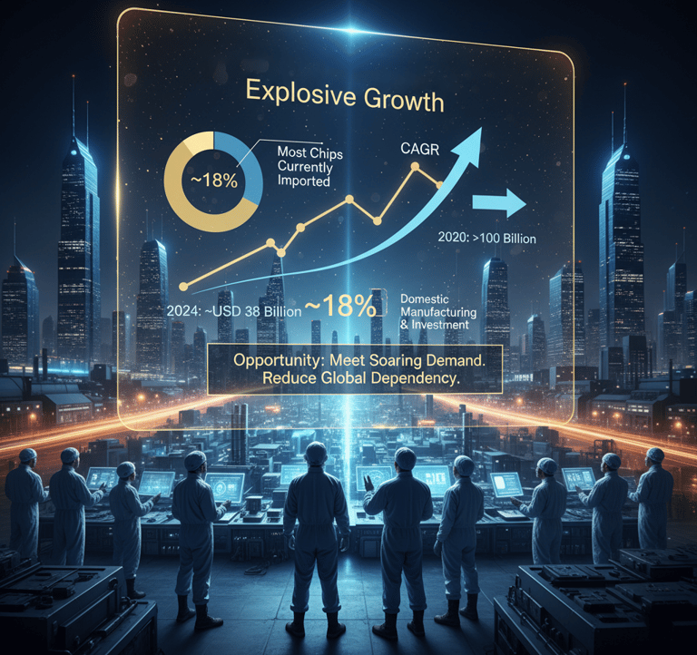
India's semiconductor market is on a trajectory of explosive growth, with forecasts projecting an expansion from as low as USD 38 billion in 2024 to as high as USD 105 billion by 2030, representing a compound annual growth rate (CAGR) of approximately 18%. Other estimates project growth to USD 103.4 billion from a 2024 base of US$ 52 billion. This surge creates a massive domestic capture opportunity, as the country currently imports the vast majority of its chips..
Korean Over-Concentration Creates Geopolitical Risk
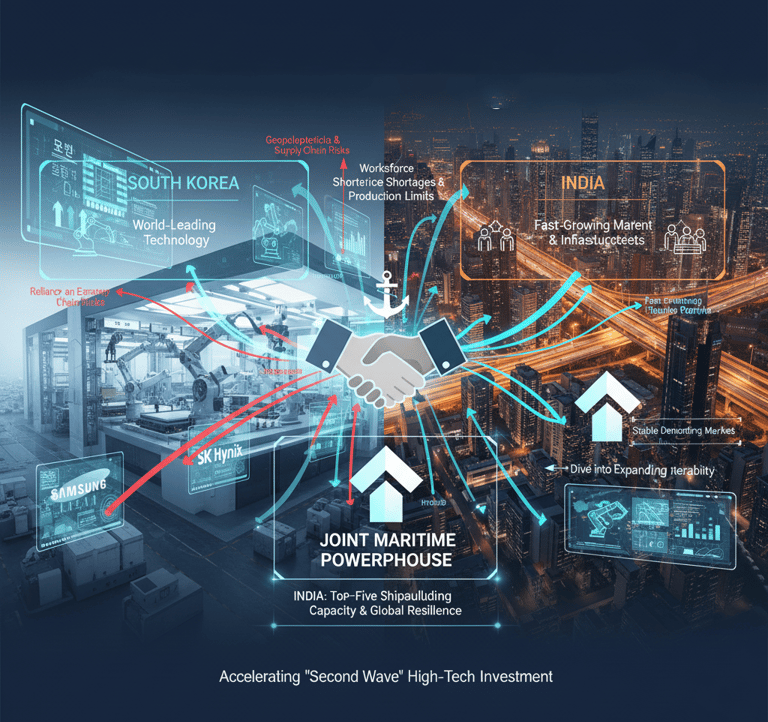
South Korean giants like Samsung and SK Hynix are global leaders, commanding significant shares of the memory market. However, this concentration presents a geopolitical vulnerability. Partnering with India, a stable democracy with aligned strategic interests, offers a critical de-risking pathway, allowing Korean firms to diversify their manufacturing footprint and secure future revenue streams in one of the world's fastest-growing economies.


Advanced Packaging Is the 4-Month Quick Win
While full-scale fabs take years to build, India can capture high-value opportunities in the mid-stream of the supply chain through advanced packaging (OSAT). Demand is soaring globally, driven by AI and high-performance computing. South Korea is a leader in advanced packaging technologies like High-Bandwidth Memory (HBM) and 2.5D/3D integration. A near-term joint venture to establish a pilot OSAT line in India represents the fastest path to revenue and ecosystem development.
The Skills Gap Is the Single-Point-of-Failure
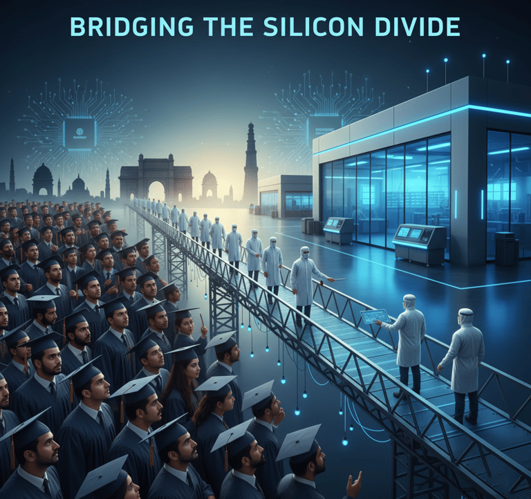
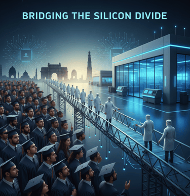
India faces a projected shortfall of 250,000-300,000 skilled semiconductor professionals by 2027. While the country produces over 1.5 million engineers annually, very few are "fab-ready," creating a critical bottleneck. The most urgent need is for hands-on talent in fabrication, packaging, and equipment maintenance. A dedicated, Korea-style hands-on training and apprenticeship hub is essential to prevent workforce shortages from delaying projects.

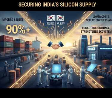
Materials Dependence Represents a Hidden Cost and Risk
India currently imports over 90% of its high-purity chemicals, specialty gases, and other critical materials for semiconductor manufacturing. This dependence creates supply chain vulnerabilities and inflates costs. Fast-tracking joint ventures with Korean materials leaders like Dongjin Semichem or LG Chem to establish local production facilities is a foundational step to de-risk the entire Indian semiconductor ecosystem..
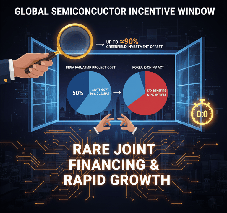
An Unprecedentedly Rich Incentive Window Is Open Now
The combination of central and state-level incentives in India creates a uniquely favorable investment climate. India's central government offers a uniform fiscal support of 50% of project costs for fabs and ATMP units. States like Gujarat add up to a 40% capital subsidy on top of this, creating a scenario where nearly 90% of greenfield fab costs can be offset. This, combined with tax credits from Korea's K-Chips Act, presents a limited-time opportunity to lock in highly favorable financing structures.
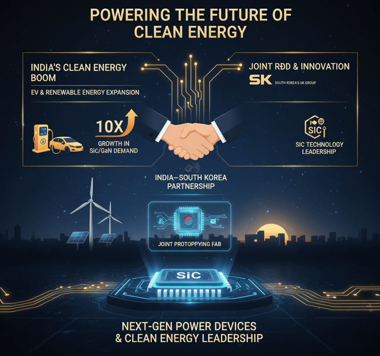
SiC/GaN Power Devices Offer a 10x Growth Niche
India's push for electric vehicles (EVs) and renewable energy is creating massive demand for wide-bandgap (WBG) semiconductors like Silicon Carbide (SiC) and Gallium Nitride (GaN). 1 South Korea's SK Group has significant capabilities in the SiC market. A joint R&D and prototyping fab for these next-generation power devices would allow the partnership to leapfrog into a high-value, high-growth market segment.
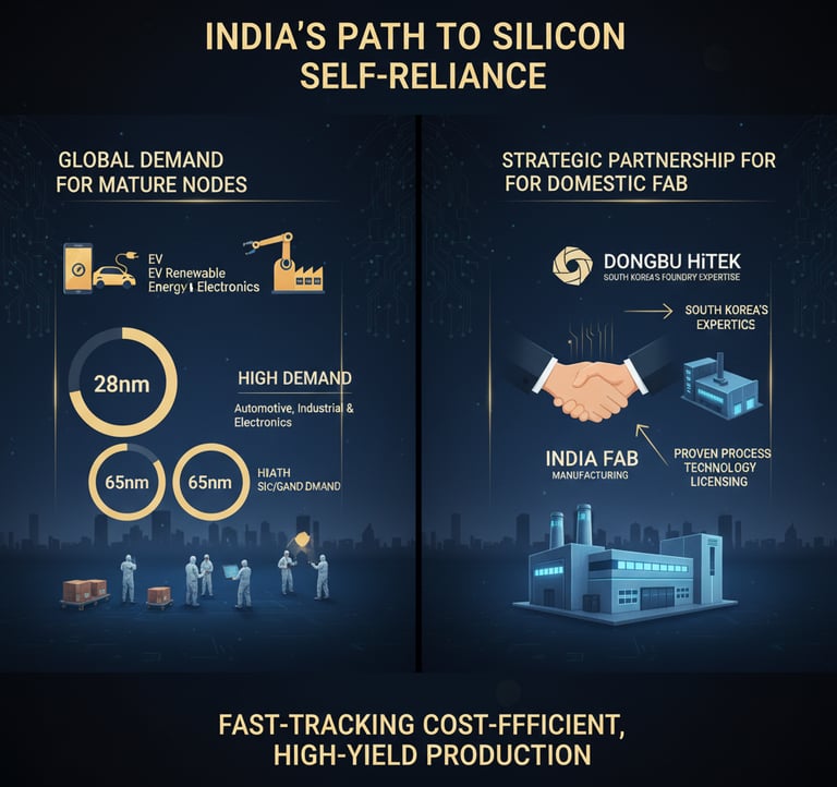
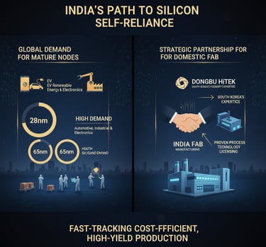
Mature-Node Fabs Remain Highly Profitable and Strategic
There is strong, sustained demand for chips built on mature nodes (e.g., 8nm, 65nm) for the automotive, industrial, and consumer electronics sectors. Establishing domestic foundry capacity at these nodes is essential for India's self-reliance. Licensing proven process technology from a South Korean partner like Dongbu HiTek can accelerate the ramp-up of a cost-effective mature-node fab in India
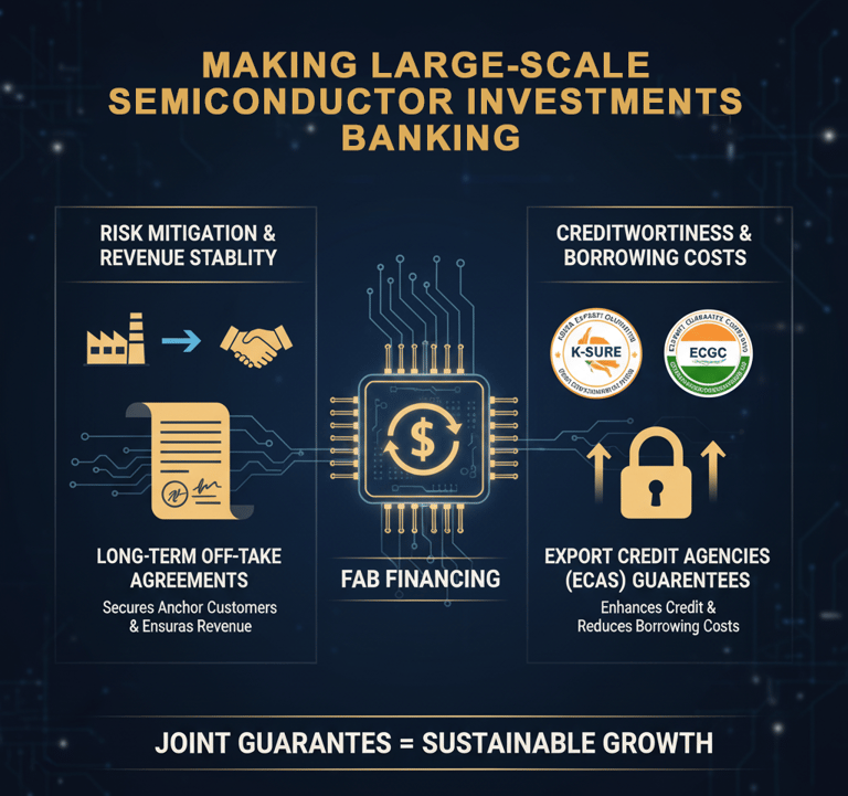
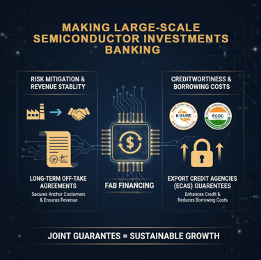
Bankability Hinges on Off-Take Agreements and Credit Enhancements
Securing financing for capital-intensive fab projects requires de-risking instruments. Long-term offtake agreements from anchor customers provide revenue certainty, a prerequisite for debt financing. Additionally, credit enhancements and guarantees from Export Credit Agencies (ECAs) like Korea's K-SURE and India's ECGC can significantly improve a project's credit profile and lower borrowing costs.
A Robust Trust Architecture Is More Critical Than Technology
Successful technology transfer hinges on a clear and comprehensive governance framework. This includes defining ownership of pre-existing (Background) and jointly created (Foreground) intellectual property. Furthermore, strict compliance with international export control regimes like the Wassenaar Arrangement and national laws is non-negotiable to prevent licensing delays and build trust. A Joint Steering Committee and clear legal structures like JVs or SPVs are essential from the outset.
Strategic Imperative:
De-Risking Asian Chips Through South Korea-India Alignment
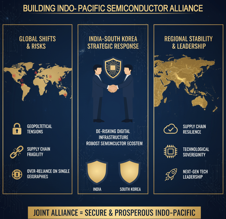
The collaboration between India and South Korea in the semiconductor domain is a strategic imperative, born from a confluence of geopolitical shifts, economic necessity, and perfectly aligned national interests. The intensifying U.S.-China technological rivalry has exposed the fragility of globally concentrated supply chains, creating an urgent need for diversification and resilience. This partnership, rooted in the Donghaeng-Manthan ethos of "walking together," offers a powerful solution by creating a secure, alternative value chain that enhances the technological sovereignty and economic security of both nations.
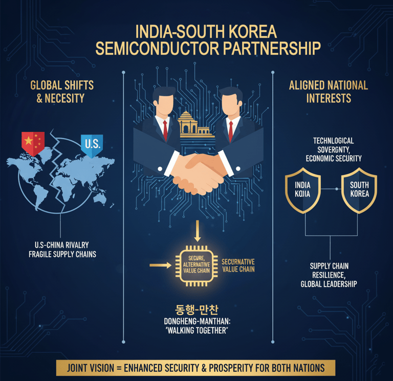
U.S.–China Tech Split Spurs Supply Diversification
The global semiconductor landscape is being reshaped by geopolitical tensions, making supply chain resilience a top priority for governments and corporations alike. For both India and South Korea, the partnership is a strategic response to de-risk their economies from over-reliance on single geographies and navigate the complexities of the 21st-century global order. By building a trusted digital infrastructure and a robust semiconductor ecosystem in the Indo-Pacific, the alliance contributes to regional stability and secures a leadership position in next-generation technology.
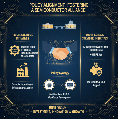
Alignment of ISM (US$10 B) and K-CHIPS (US$450 B) Incentives
The strategic vision is underpinned by powerful, state-backed policy alignment. India's ambitious $10 billion India Semiconductor Mission (ISM) and 'Make in India' initiative are perfectly complemented by South Korea's massive $450 billion 'K-Semiconductor Belt' strategy and the 'K-CHIPS Act'. These initiatives create a fertile ground for collaboration, with both governments providing substantial financial incentives, tax credits, and infrastructure support to foster investment in R&D, fabrication, and packaging. This policy synergy is reinforced by institutional momentum, such as the MoU between the India Electronics and Semiconductor Association (IESA) and the Korea Display Industry Association (KDIA) for joint R&D and workforce development.

Mutual Benefits Matrix — Market Access vs. Manufacturing Mastery
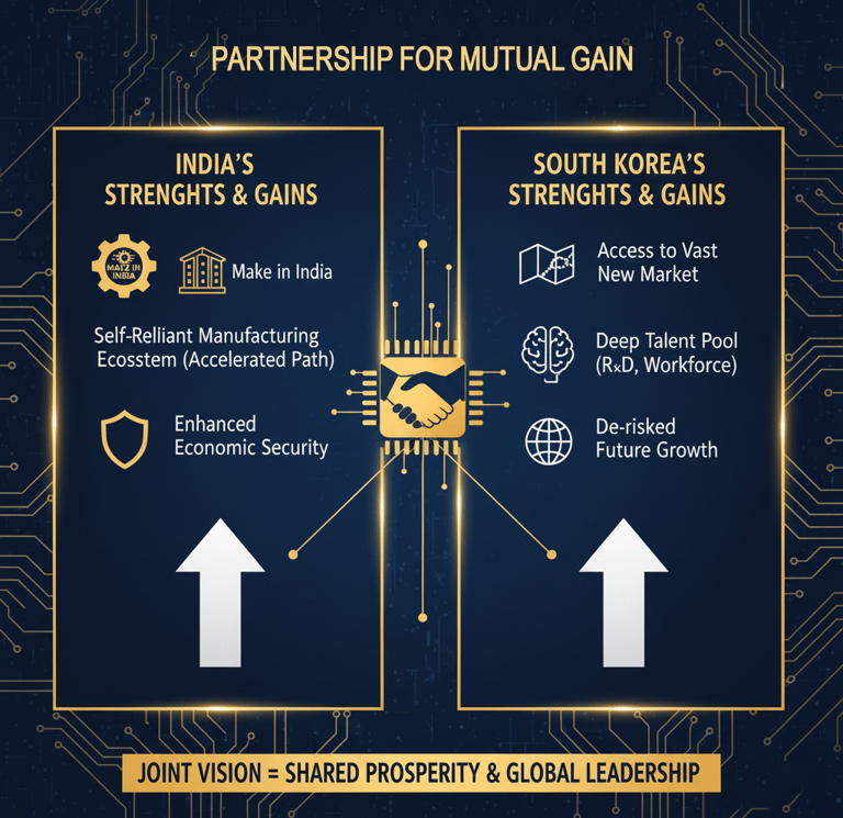
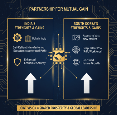
The partnership is fundamentally symbiotic, allowing each nation to leverage its unique strengths for mutual gain. India gains an accelerated path to building a self-reliant manufacturing ecosystem, while South Korea gains access to a vast new market and a deep talent pool, effectively de-risking its future growth.
For India
Benefit Category
For South Korea
Technology & Expertise = Access to world-class precision engineering, cutting-edge manufacturing processes (memory, packaging, foundry), and decades of ecosystem-building expertise.
Market Access = Opportunity to move up the global technology value chain and reduce import dependency for a domestic market projected to exceed $100B.
Supply Chain & Geopolitics = Development of a self-reliant, resilient domestic semiconductor hub, enhancing national and economic security.
Capital & Investment = Inflow of significant capital investment from Korean corporations, accelerated by robust government incentives.
Technology & Expertise = Access to India's immense pool of skilled design and software engineers at a competitive cost, fueling innovation in areas like AI chip design.
Market Access = Strategic access to India's vast and rapidly expanding market, especially in high-growth sectors like EVs, 5G, and AI, securing future revenue streams.
Supply Chain & Geopolitics = Diversification of global supply chains away from geopolitically sensitive regions, mitigating risk by investing in a stable, investment-friendly democracy.
Capital & Investment = Opportunity to leverage attractive Indian government incentives (e.g., PLI schemes) to de-risk and enhance the ROI of new manufacturing investments.
This powerful synergy enables India to build its manufacturing muscle while South Korea secures its future markets, creating a formidable alliance in the global tech landscape.
India Demand Deep-Dive:
Where the US$105 B Will Land
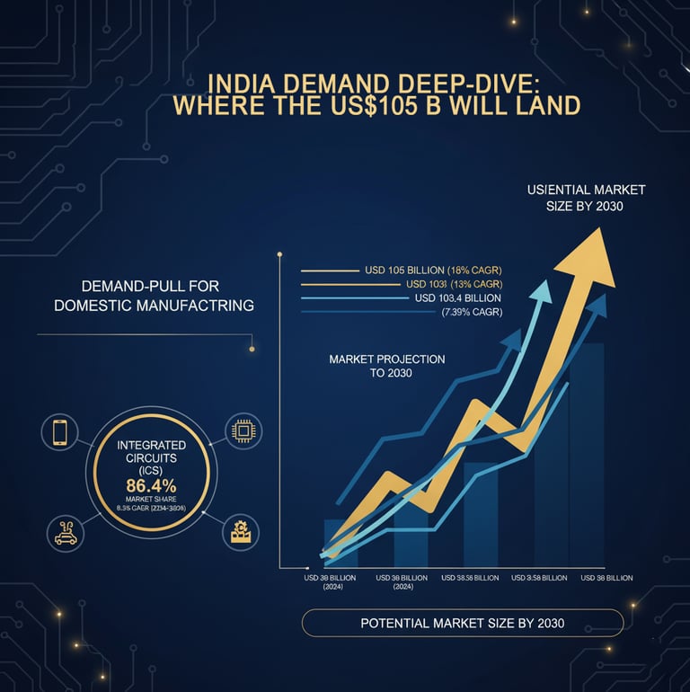
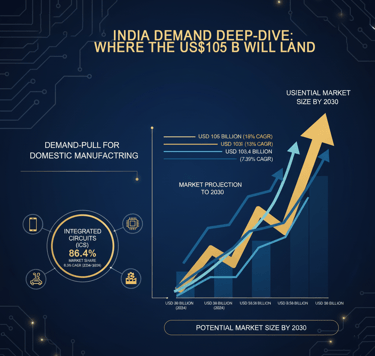
India's semiconductor market is poised for exponential growth, creating a powerful demand-pull for domestic manufacturing. Integrated Circuits (ICs) are the dominant device category, accounting for a commanding 86.4% of total market revenue in 2024 and projected to grow at a CAGR of 8.3% through 2030. While forecasts vary, the trajectory is clear: the market is projected to surge from a 2024 baseline of USD 38 billion to as high as USD 105 billion by 2030, implying an 18% CAGR. Other analyses project growth from US$ 52 billion in 2024 to US$ 103.4 billion by 2030 (13% CAGR) or a more conservative expansion from USD 13.54 billion in 2025 to USD 23.58 billion by 2030 (7.39% CAGR).
Sector Hot-Spots — 5G, AI Data Centers, and EVs
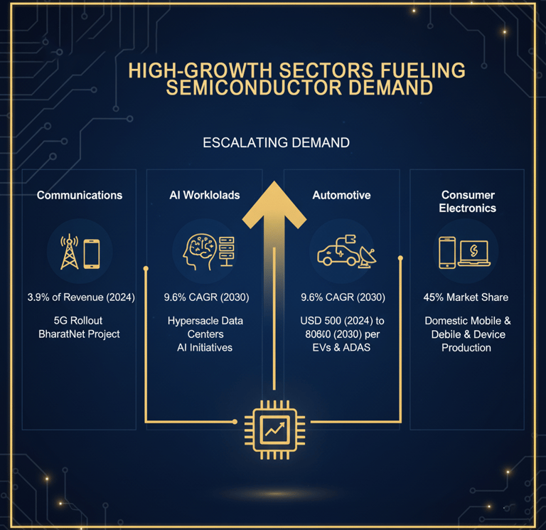
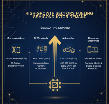
This escalating demand is fueled by several key high-growth sectors:
Communications: This sector is a primary driver, accounting for 32.9% of revenue in 2024, propelled by the nationwide 5G rollout and the expansive BharatNet project.
AI Workloads: The rise of AI is fueling a 9.6% CAGR in demand through 2030, driven by the construction of hyperscale data centers and government-led AI initiatives.
Automotive: The automotive sector is rapidly digitizing, with the semiconductor content per vehicle expected to increase from USD 500 in 2024 to USD 800 by 2030, largely due to the push for Electric Vehicles (EVs) and Advanced Driver-Assistance Systems (ADAS).
Consumer Electronics: This remains the largest application segment with a 45% market share, driven by the domestic production of mobile handsets and other devices.
Device Mix Forecast — ICs vs. Discrete/Opto/Sensors
While Integrated Circuits dominate the market, other device categories are also poised for growth in alignment with national priorities.
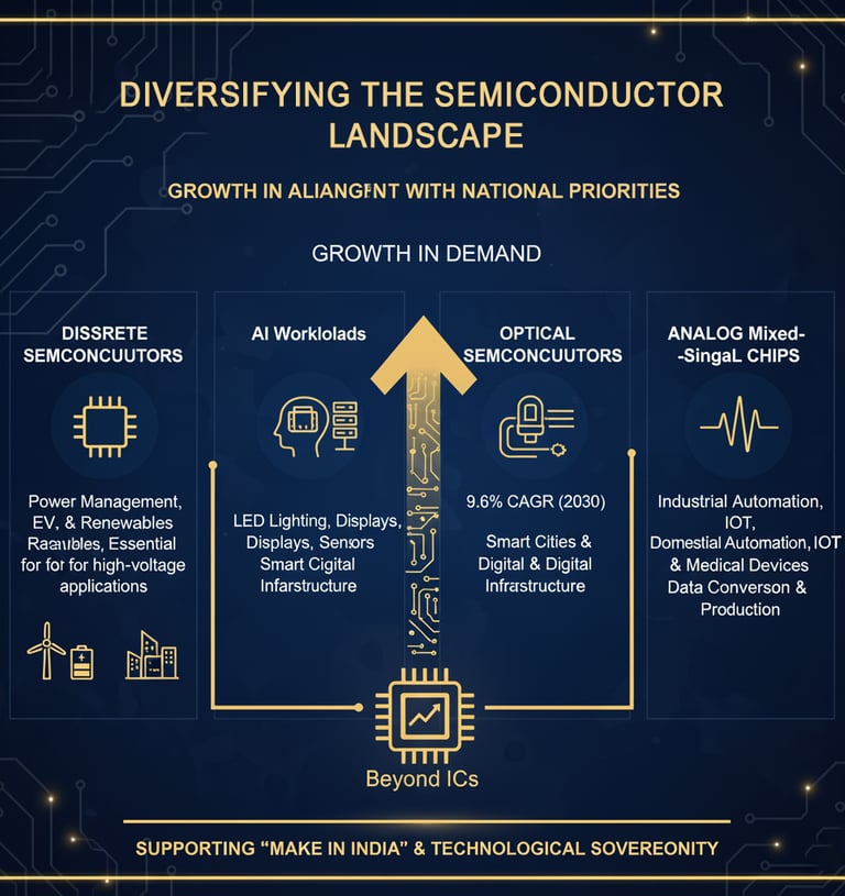
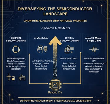
Device Type = Integrated Circuits (ICs)
2024 Market Share = 86.4%
Projected CAGR (2024-2030) = 8.3%
Key Drivers = Mobile, AI, Automotive, 5G
Device Type = Discrete Devices
2024 Market Share = Smaller Share
Projected CAGR (2024-2030) = Poised for Growth
Key Drivers = Power Electronics, EVs
Device Type = Optoelectronics
2024 Market Share = Smaller Share
Projected CAGR (2024-030) = Poised for Growth
Key Drivers = Displays, Communications
Device Type = Sensors
2024 Market Share = Smaller Share
Projected CAGR (2024-2030) = Poised for Growth
Key Drivers = Industrial IoT, Automotive
Note: Data for this table is synthesized from the research context, which specifies IC dominance and notes growth potential in other categories.
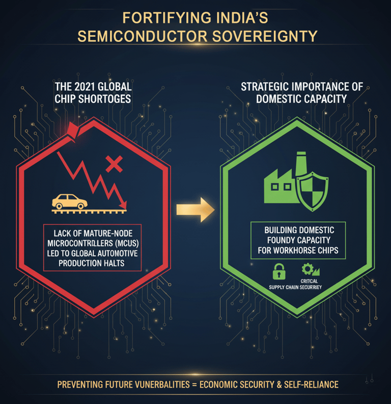
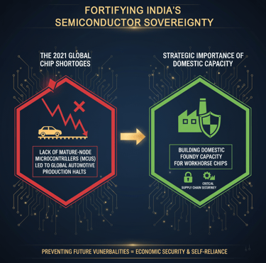
Failure Case — 2021 Automotive MCU Shortages
The strategic importance of domestic capacity was starkly illustrated during the global chip shortages of 2021, which severely impacted the automotive industry. A lack of mature-node microcontrollers (MCUs) forced production halts for major car manufacturers worldwide. Building domestic foundry capacity for these workhorse chips is not just an economic opportunity but a crucial step to prevent such vulnerabilities in the future and ensure supply chain security for India's critical industries.
South Korea’s Exportable Strengths vs. India’s Gaps
The foundation of the Donghaeng-Manthan vision is the complementary nature of the two nations' ecosystems. South Korea brings a deep well of manufacturing mastery and technological leadership, while India offers a burgeoning design ecosystem and immense scale. This synergy allows for a direct mapping of Korean capabilities to address India's most critical gaps in its journey toward semiconductor self-reliance.
Korean Capability = Memory Chips (DRAM/NAND)
Global Position / Key Strength = Global leader; Samsung & SK hynix hold >70% DRAM share.
Indian Gap = No at-scale memory fabrication.
Proposed JV/Transfer Model = Greenfield Fab JV: Transfer high-volume manufacturing best practices.
Korean Capability = Advanced Packaging (OSAT)
Global Position / Key Strength = World-class expertise in HBM, 2.5D/3D, FOWLP.
Indian Gap = Nascent ecosystem; no high-volume .2.5D/3D lines.
Proposed JV/Transfer Model = OSAT JV: Partner with Hana Micron or Nepes to build pilot lines.
Korean Capability = Semiconductor Materials & Chemicals
Global Position / Key Strength = Robust domestic industry for photoresists, CMP slurries, specialty gases.
Indian Gap = Over 90% of critical materials are imported.
Proposed JV/Transfer Model = OSAT JV: Local Plant JV: License purification tech from Dongjin Semichem or LG Chem.
Korean Capability = Semiconductor Equipment & MRO
Global Position / Key Strength = Strong base of equipment makers (Hanmi, Wonik) and maintenance expertise.
Indian Gap = High dependence on foreign OEMs for service, leading to downtime..
Proposed JV/Transfer Model = Service Hubs: Establish local MRO centers to reduce fab downtime.
Korean Capability = Compound Semiconductors (SiC/GaN)
Global Position / Key Strength = Growing capabilities in WBG materials, led by SK Group. Indian Gap = Nascent R&D and fabrication efforts.
Proposed JV/Transfer Model = R&D Proto Fab: Collaborate on SiC/GaN device fabrication for EV market.
Korean Capability = Mature-Node Foundry Operations
Global Position / Key Strength = Deep expertise in high-yield, cost-effective 28-65nm fabs (e.g., Dongbu HiTek).
Indian Gap = Fabs are planned but not yet operational..
Proposed JV/Transfer Model = Technology Licensing: Transfer PDKs and operational best practices.
This direct alignment forms a blueprint for targeted collaboration, enabling India to systematically build a vertically integrated supply chain by leveraging proven Korean technology and operational excellence.
High-Impact Collaboration Plays
To maximize immediate impact and build long-term strategic advantage, the collaboration should prioritize four high-leverage areas. These plays are selected based on their potential for rapid return on investment, significant ecosystem uplift, and alignment with India's most pressing market demands.
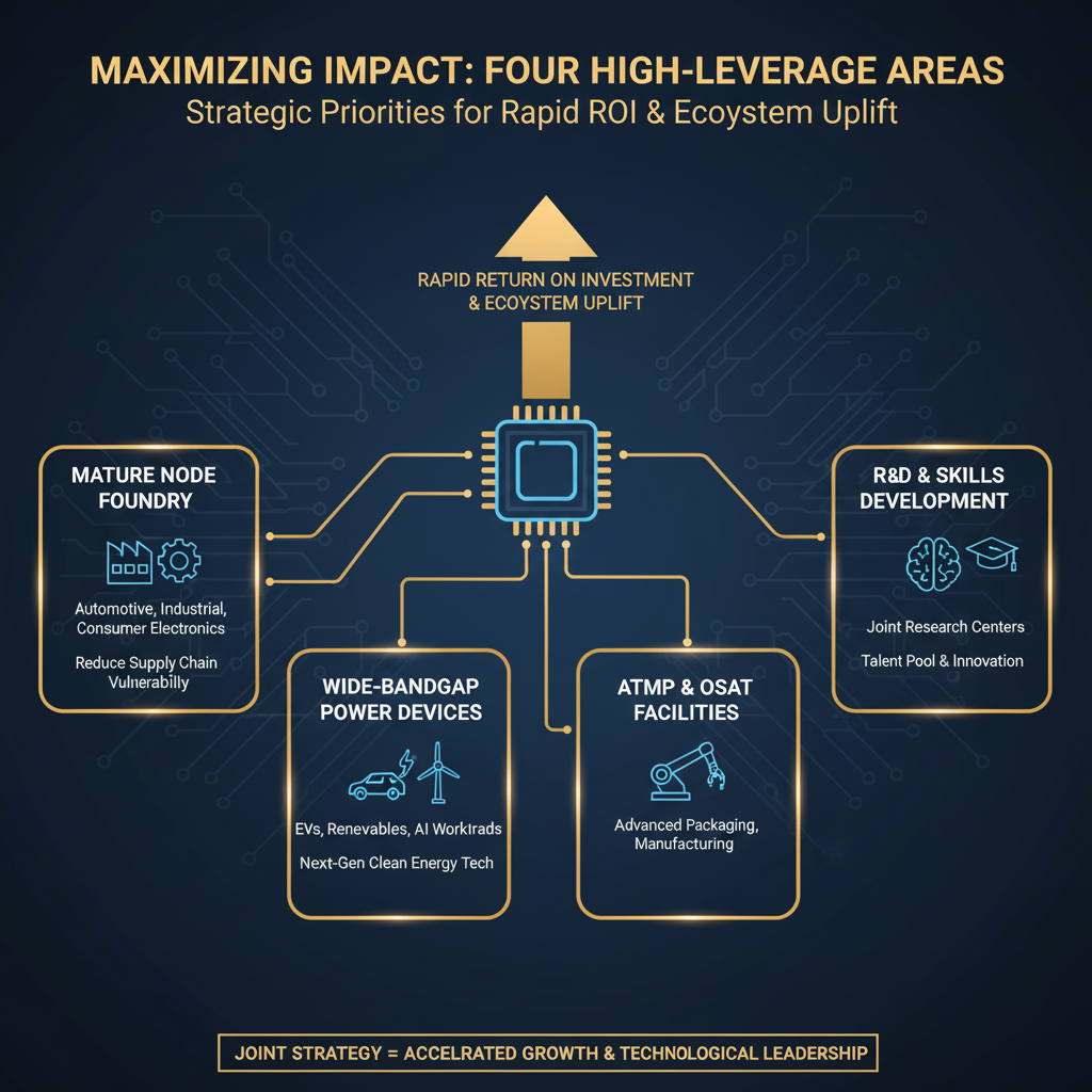
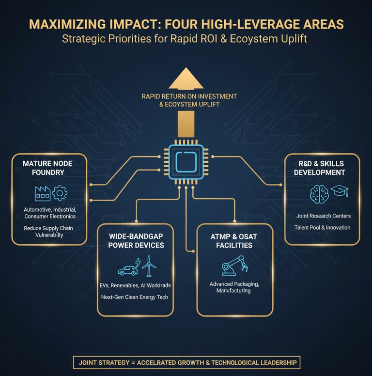
Advanced Packaging Pilot — The Quickest Path to Value
Establishing an advanced packaging (OSAT) facility offers the highest immediate leverage. It allows India to capture a high-value step in the supply chain for AI, HPC, and automotive chips while its full-scale fabs are under construction.With Korean leaders like Samsung, SK hynix, and Hana Micron providing technology transfer for 2.5D/3D integration, a pilot line could be established with a 24-month timeline, targeting the exponentially growing domestic demand for packaged chips.
Chemicals Localization — De-Risking the Entire Ecosystem
Localizing the production of specialty gases and ultrapure wet chemicals is a foundational imperative. It directly addresses India's critical import dependency and enhances the operational stability and cost-effectiveness of all current and future fab projects. A joint venture with a sophisticated Korean chemical supplier could reduce wafer costs by an estimated 8-12% and mitigate the risk of supply disruptions, as seen in past geopolitical disputes. The global market for these chemicals is projected to hit USD 29.3 billion by 2030, making localization a significant economic opportunity.
SiC/GaN Power Devices — Capturing the EV Revolution
This niche offers exceptionally high growth potential, directly fueled by India's aggressive EV adoption targets. With India's EV market poised for explosive growth, the demand for SiC/GaN power management ICs and MOSFETs represents a multi-billion dollar import substitution opportunity. Partnering with Korean firms like SK Group, which has a strategic interest in the SiC market, can help India leapfrog into this next-generation technology and establish a leadership position.
Mature-Node Foundry — Securing Foundational Supply
There is strong and sustained demand for chips on mature nodes (8nm, 40nm) from India's automotive, industrial IoT, and consumer electronics sectors. Establishing domestic foundry capacity is essential for self-reliance. The automotive sector alone is a major driver, with semiconductor content per vehicle projected to rise significantly. A technology partnership with a Korean foundry expert can de-risk the complex process of fab construction and accelerate the ramp-up to high-yield production, securing the supply of foundational components like MCUs and PMICs.
Pilot Project Portfolio & Timeline
The Donghaeng-Manthan mission is best realized through a phased portfolio of pilot projects, sequenced to build capabilities incrementally and generate momentum. This approach balances near-term wins with long-cycle flagship investments, ensuring sustainable growth.
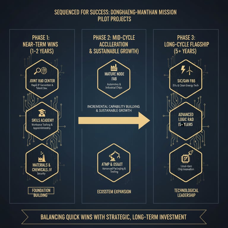
Phase = Near-Term (≤6 mo)
Project = Workforce Training Hub
Est. CapEx = $0.5–3M
Go-Live = 6 mo
Key Performance Indicator (KPI) = 500-1,000 certified trainees/year
Potential Korean Lead = Samsung, SK Hynix
Potential Indian Lead = MeitY (C2S Program), IESA, IITs
Phase = Mid-Term (12–24 mo)
Project = Advanced Packaging & OSAT Pilot Line
Est. CapEx = $5–30M
Go-Live = 24 mo
Key Performance Indicator (KPI) = 10k–50k units/day capacity
Potential Korean Lead = Amkor Korea, APACT Co.
Potential Indian Lead = Tata Electronics, Foxconn India
Phase = Mid-Term (12–24 mo)
Project = Specialized Materials & Chemicals Plant
Est. CapEx = $10–50M
Go-Live = 24 mo
Key Performance Indicator (KPI) = 2-3 critical materials qualified
Potential Korean Lead = LG Chem, Dongjin Semichem
Potential Indian Lead = Reliance Industries, Tata Group
Phase = Flagship (36–60 mo)
Project = 200mm Mature Node Pilot Fab (65/90nm)
Est. CapEx = $50–100M
Go-Live = 48 mo
Key Performance Indicator (KPI) = 5k–10k Wafer Starts Per Month (WSPM)
Potential Korean Lead = Dongbu HiTek
Potential Indian Lead = Tata Electronics, State Govts.
Phase = Flagship (36–60 mo)
Project = Prototype Fab for Power Electronics (GaN/SiC)
Est. CapEx = $10–100M
Go-Live = 60 mo
Key Performance Indicator (KPI) = 20+ patents filed, new device prototypes
Potential Korean Lead = KAIST/KIST, SK Group
Potential Indian Lead = IISc/IITs, C-MET
Note: Data for this table is synthesized from the proposed_pilot_projects research data.
This staggered approach allows foundational pillars like talent and design to be established first, paving the way for more complex manufacturing and supply chain projects.
Talent Pipeline Blueprint: Closing the 300k Gap
Addressing India's critical semiconductor skills gap is the most urgent prerequisite for success. A multi-pronged strategy focusing on practical, hands-on training is required to transform India's vast pool of engineering graduates into a fab-ready workforce.
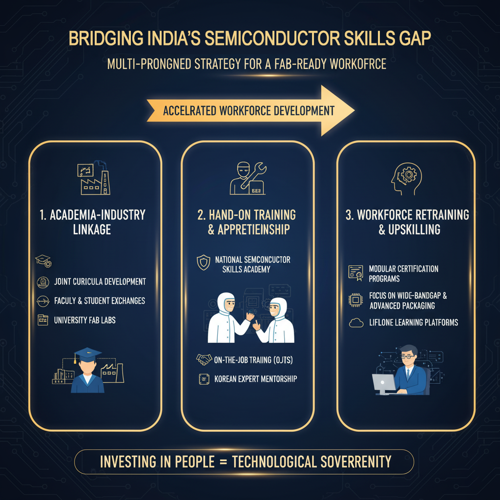
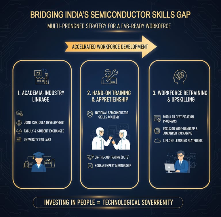
Government-Led Initiatives and Curriculum Co-Design with South Korea

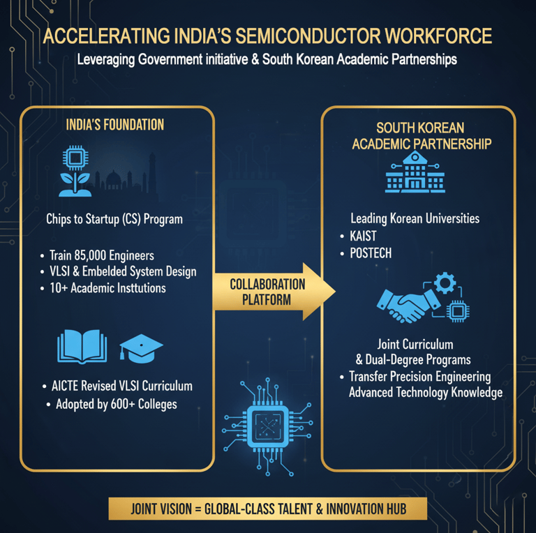
The Indian government has already laid the groundwork with key initiatives. The 'Chips to Startup' (C2S) Program aims to train 85,000 engineers in VLSI and Embedded System Design across 120 academic institutions. This provides a perfect platform for collaboration. By partnering with leading Korean universities like KAIST and POSTECH, joint curricula and dual-degree programs can be developed to transfer precision engineering knowledge directly. This effort is complemented by the AICTE's revised VLSI curriculum, already adopted by over 600 colleges.
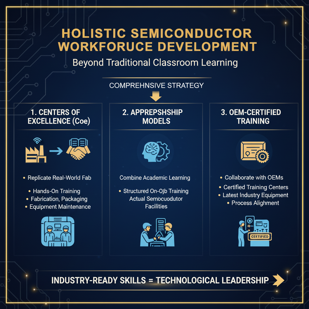
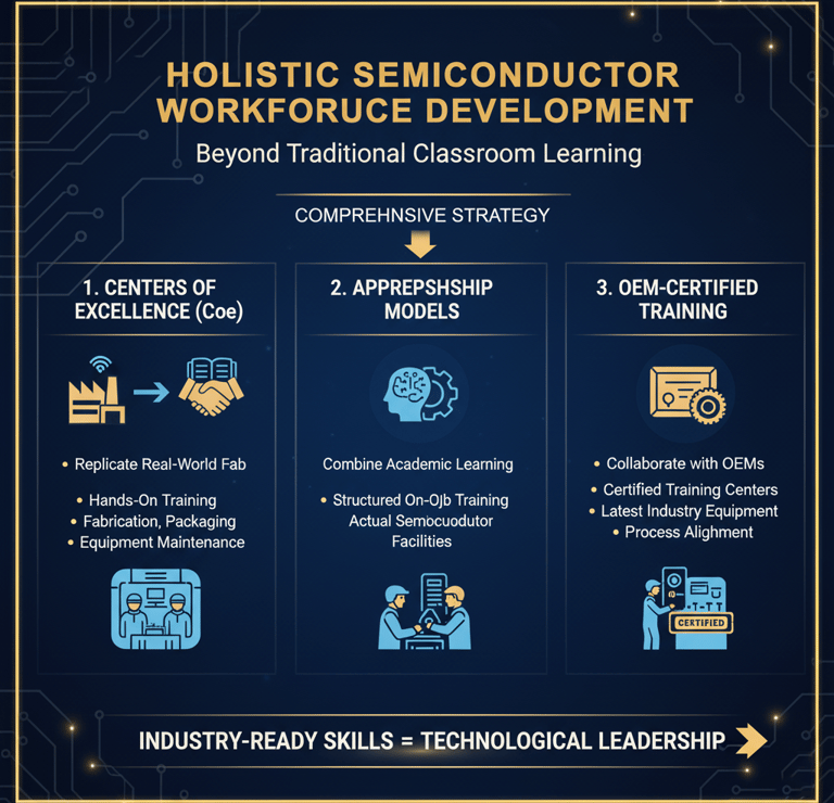
Hands-on CoEs, Apprenticeships, and OEM-Certified Training
Classroom learning alone is insufficient. The strategy must include:
Centers of Excellence (CoEs): Establishing CoEs that replicate real-world fab environments for hands-on training in fabrication, packaging, and equipment maintenance.
Apprenticeship Models: Implementing robust apprenticeship programs that combine academic learning with structured on-the-job training in actual semiconductor facilities.
OEM-Certified Training: Collaborating with Original Equipment Manufacturers (OEMs) to create certified training centers, ensuring skills are aligned with the latest industry equipment and processes.
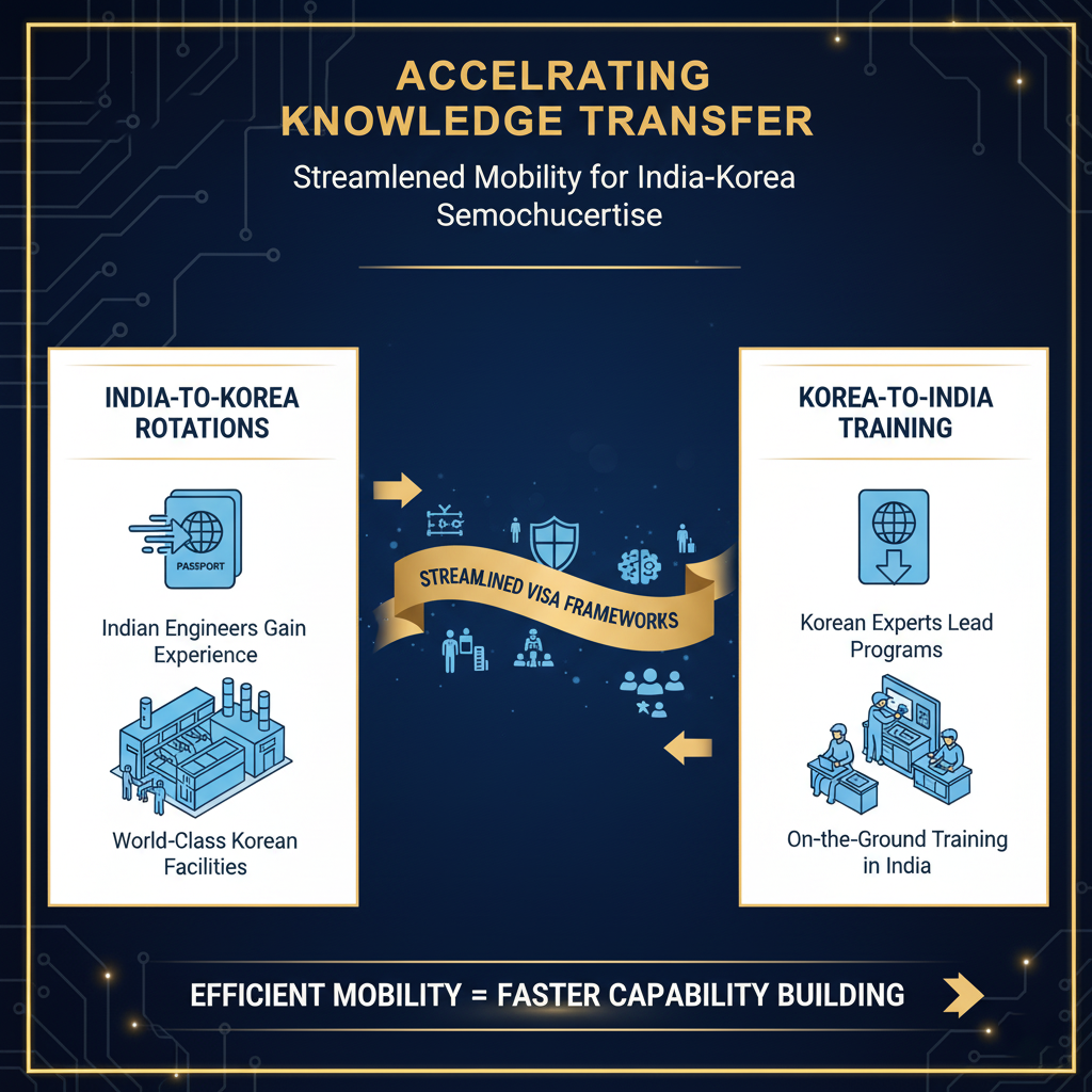

Facilitating Workforce Mobility
To accelerate knowledge transfer, streamlined visa frameworks should be advocated for. This would facilitate Korea-India rotations, allowing Indian engineers to gain invaluable experience in world-class Korean facilities while enabling Korean experts to lead training programs on the ground in India.
Incentive & Financing Stack:
From CapEx Subsidies to Blended Debt
Financing capital-intensive semiconductor projects requires a sophisticated, multi-layered approach that leverages the uniquely favorable incentive structures offered by both India and South Korea.
The Power of Layered Central & State Incentives
India's policy framework is designed to significantly de-risk capital expenditure. The central government's India Semiconductor Mission (ISM) provides a foundational fiscal support of 50% of the project cost on a pari-passu basis for approved fabs and ATMP units. This is then amplified by aggressive state-level incentives.
State with Key Incentives
Gujarat = 40% additional capital subsidy; 75% subsidy on first 200 acres of land; full stamp duty reimbursement; discounted power/water.
Tamil Nadu = State capital subsidy up to 50% of the central incentive; concessional land; full exemption on stamp duty and electricity tax.
Uttar Pradesh = 50% additional capital subsidy over central support; extensive tax exemptions and land rebates.
Andhra Pradesh = Capital subsidy equal to 60% of the central incentive; training subsidies.
This layered approach can offset a substantial portion of initial project costs, dramatically improving the project's ROI and lowering the hurdle for private investment.
Structuring the Capital Stack
A typical capital stack for a fab project combines public and private funding sources to balance risk and returns over a long-term horizon.
Government Incentives: This forms the foundational layer, comprising direct fiscal support from India's ISM and tax credits from South Korea's K-Chips Act. This layer significantly reduces the total capital required from private sources.
Equity: This includes sponsor equity from anchor corporate investors (e.g., Tata, Samsung) and potentially third-party equity from financial investors or sovereign wealth funds (e.g., NIIF, Korea Investment Corporation).
Debt: This layer consists of senior and subordinated debt from commercial banks and Development Finance Institutions (DFIs). The bankability of this debt is heavily dependent on the security provided by government incentives and risk-sharing instruments.
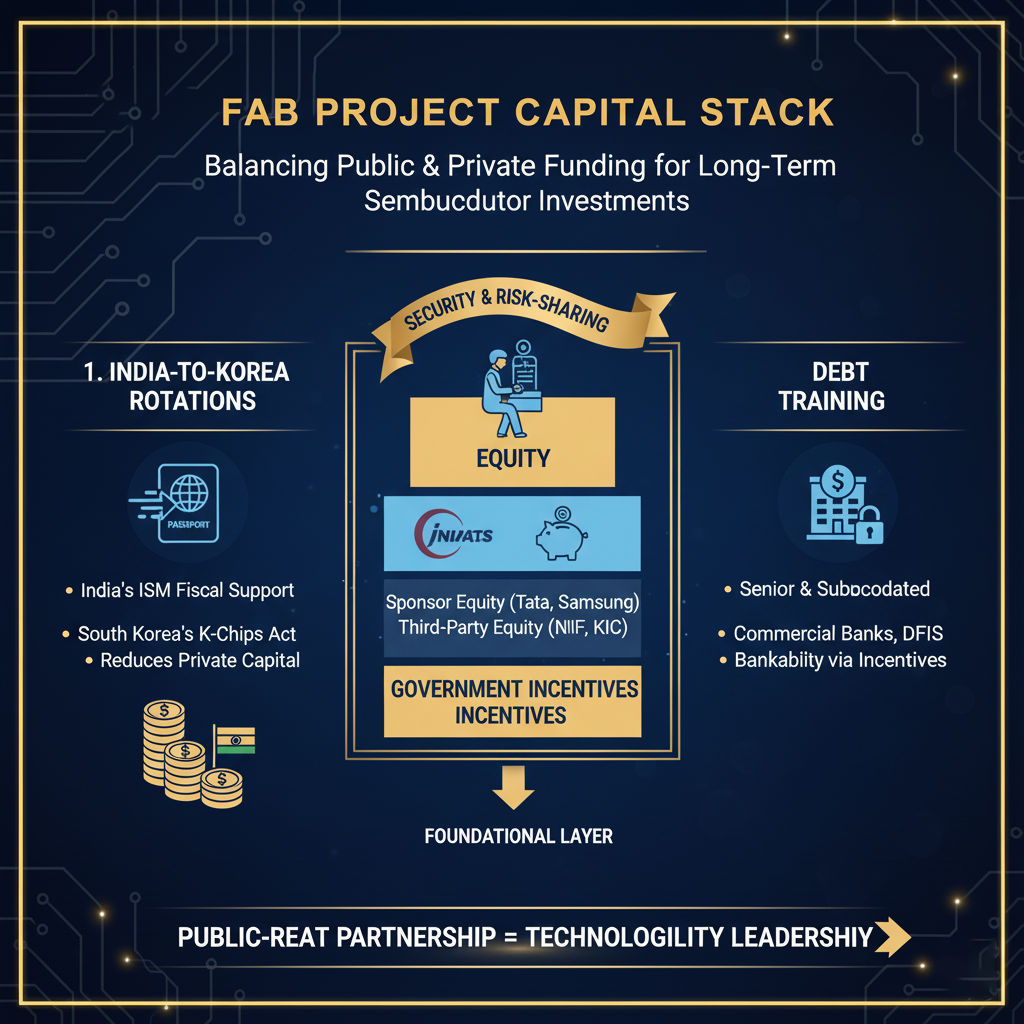
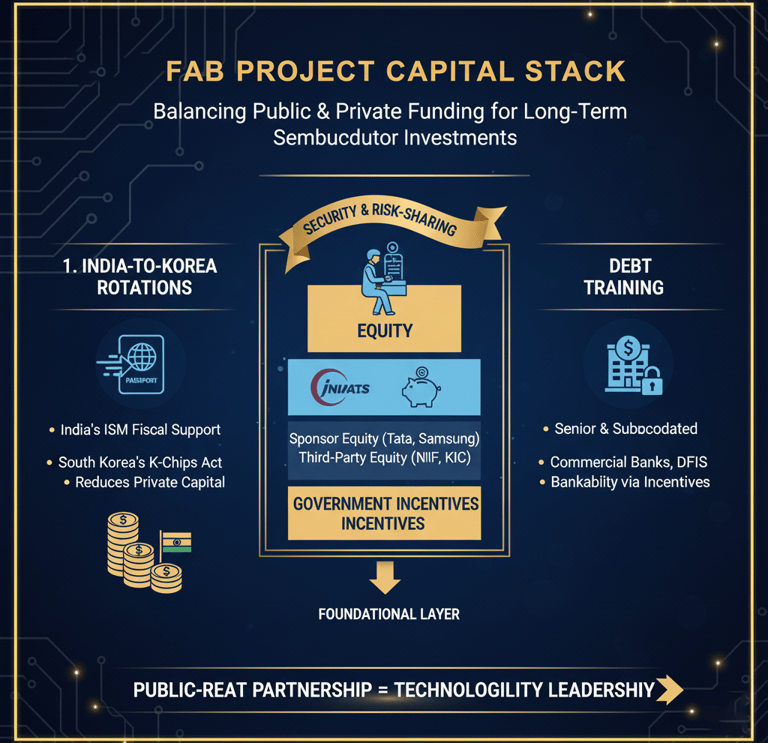
Essential Risk-Sharing Instruments
To make projects 'bankable' and attract private debt, several instruments are crucial:
Offtake Agreements: Long-term purchase guarantees from anchor customers provide revenue certainty.
MRL/TRL-Linked Disbursement: Structuring financing in tranches tied to achieving specific Manufacturing or Technology Readiness Levels ensures capital is deployed as the project matures and de-risks.
Credit Insurance & Guarantees: Instruments from Export Credit Agencies (ECAs) like India's ECGC and Korea's K-SURE, or multilateral agencies, protect against political and credit risks, enhancing project creditworthiness.
Governance & IP Protection Framework
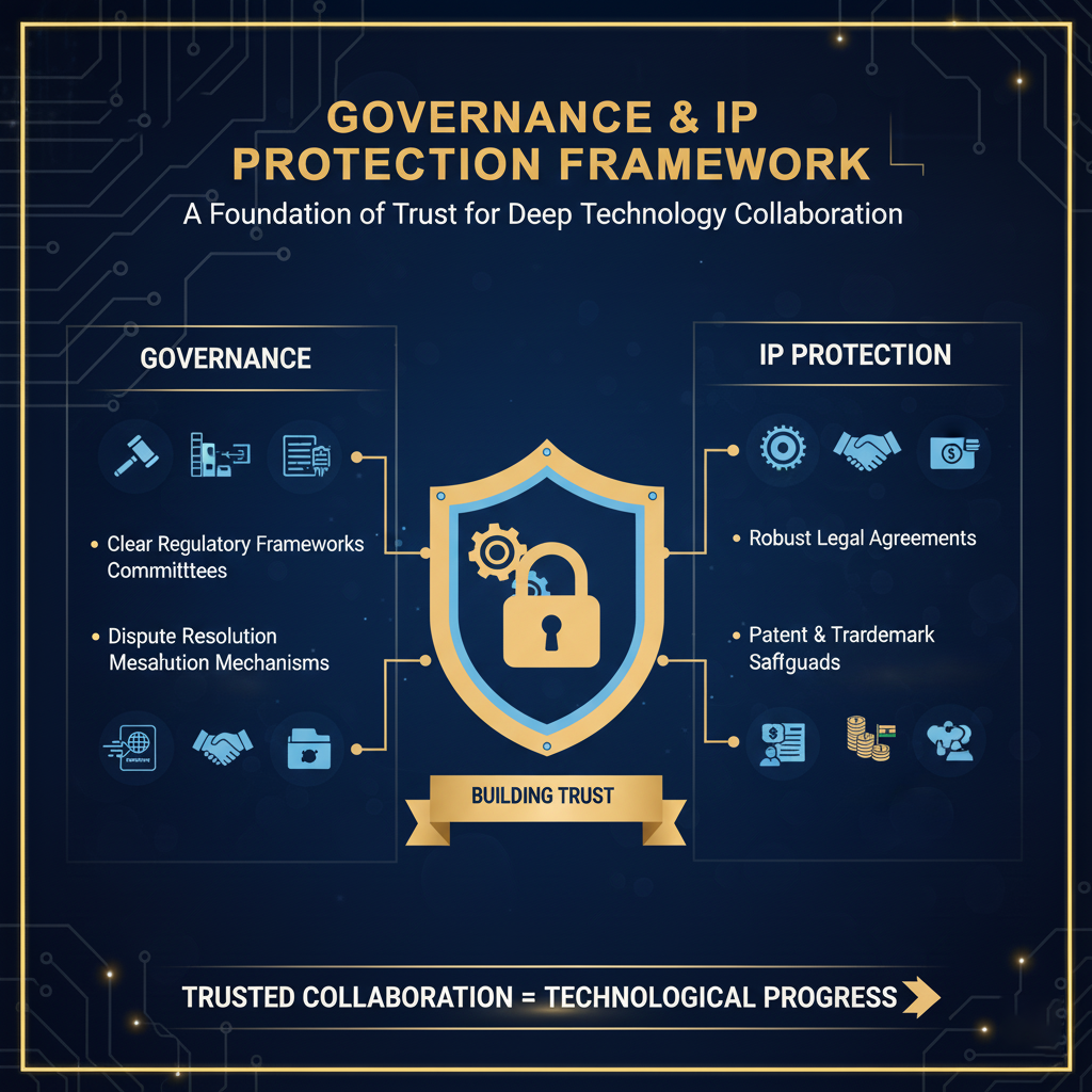
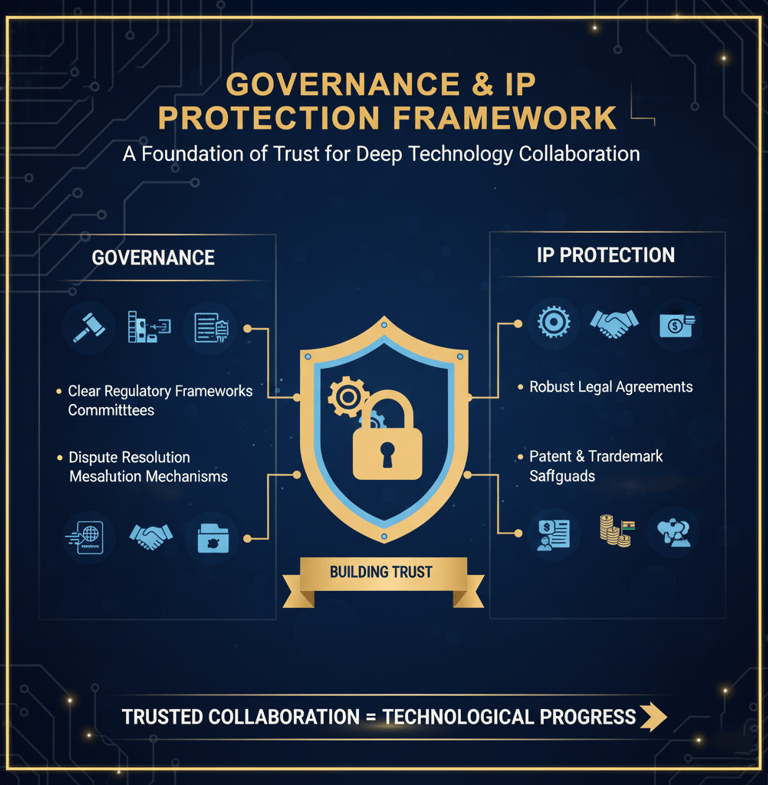
A Multi-Layered Governance Model
A robust cross-border governance structure is proposed to provide strategic direction and operational oversight:
Joint Steering Committee: A high-level body with representatives from India's MeitY, Korea's MOTIE, and key industry partners to set strategy and resolve roadblocks.
Cross-Border Program Management Office (PMO): A dedicated team to manage day-to-day project coordination, execution, and KPI monitoring.
Technical Advisory Boards: Composed of semiconductor experts to provide technical guidance and validate technology choices.
A foundation of trust, enabled by clear governance and robust IP protection, is essential for the success of this deep technology collaboration.
Recommended Legal Structures for Collaboration
The choice of legal structure should be tailored to the project's scope:
Joint Ventures (JVs): The preferred model for large-scale fabs and OSAT facilities, allowing partners to share risks, capital, and profits while combining complementary strengths.
Special Purpose Vehicles (SPVs): Ideal for financing large projects, as an SPV legally separates the project's financial risk from the parent companies.
Technology Licensing Agreements: An effective model for transferring specific, well-defined process technologies or IP in exchange for royalties or fees.
A Clear Framework for Intellectual Property
A comprehensive IP governance framework is paramount. Agreements must clearly delineate ownership of both 'Background IP' (pre-existing) and 'Foreground IP' (newly created). The framework must also define licensing terms, commercialization rights, and robust protocols for confidentiality and data protection to foster trust and encourage technology transfer.
Risk Radar & Mitigation Playbook
While the opportunity is immense, the path to establishing a semiconductor ecosystem is fraught with challenges. Proactive risk management is critical.
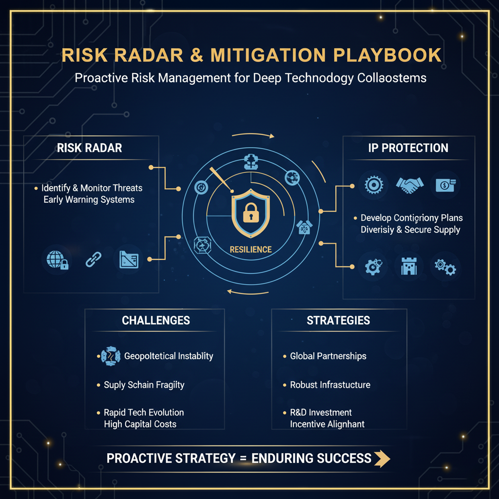
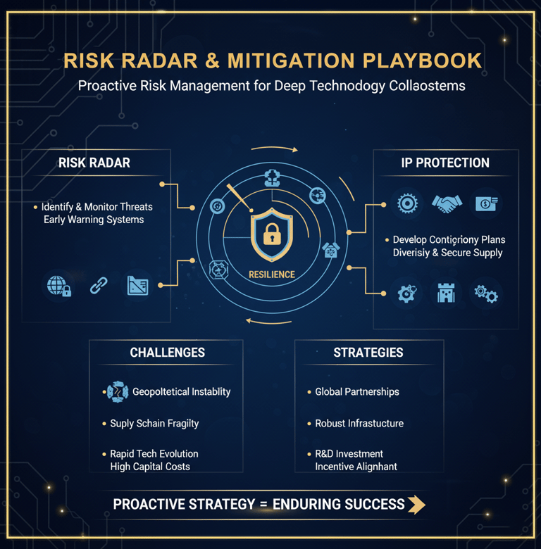
Workforce Shortage: The Primary Bottleneck
Risk: A projected shortfall of up to 300,000 skilled professionals by 2027 could severely delay project timelines and hinder operational efficiency.
Mitigation: Immediately launch the proposed Semiconductor Workforce Training & Skill Development Hub.Leverage government programs like C2S and foster industry-academia partnerships to create a pipeline of fab-ready talent
Utility Infrastructure: The Achilles' Heel of Fabs
Risk: Fabs require massive amounts of ultrapure water and an uninterrupted, highly stable power supply. Lack of this infrastructure can inflate project capex by 15-20% and cause costly operational disruptions.
Mitigation: Prioritize site selection in states like Gujarat that offer dedicated 'Semicon Cities' with ready-built utility corridors and substantial subsidies (e.g., 75% on land) to offset infrastructure costs.
Export Controls and Regulatory Compliance
Risk: Semiconductor technology is subject to strict export controls, including the Wassenaar Arrangement (to which both India and Korea are signatories) and potentially U.S. Export Administration Regulations (EAR) if US-origin tech is involved. Failure to comply can result in severe penalties and project halts.
Mitigation: Establish a compliance function within the governance model to conduct thorough due diligence on technology origin and proactively engage with regulatory authorities (e.g., Korea's MOTIE) to secure necessary export licenses early in the project lifecycle.
Success Metrics & KPI Dashboard
To ensure the Donghaeng-Manthan mission remains on track, progress must be measured against a clear set of Key Performance Indicators (KPIs) that track value creation across different time horizons.

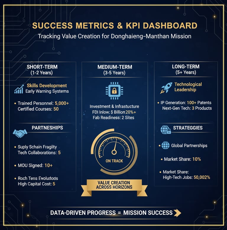
Short-Term (6–24 months): Foundational Capability Building
Talent: Number of trainees certified by the Workforce Hub annually (Target: 500-1,000).
Packaging: Daily packaging capacity of the OSAT pilot line (Target: 10,000-50,000 units).
Partnerships: Number of joint R&D projects initiated between Korean and Indian institutions
Mid-Term (24–48 months): Ecosystem Maturation
Localization: Percentage of critical semiconductor materials localized (Target: Reduce import share).
Yield & Quality: Process yield percentage and defect rate (PPM) achieved in pilot lines.
Innovation: Number of patents filed from joint R&D collaborations.
Long-Term (60+ months): Strategic & Economic Impact
Import Substitution: Total value of semiconductor imports substituted by domestic production.
Fab Performance: Wafer starts per month (WSPM) and cost-per-wafer at flagship fabs.
Financial Return: Return on Investment (ROI) and payback period for joint venture projects.
Join us in sustainable innovation efforts.
Engage
Support
© Donghaeng-manthan 2025. All rights reserved.